From Sand to Silicon: How Semiconductor Chips Are Made and the Future of Manufacturing
Learn how semiconductor chips are made from sand, the photolithography process, and what's next in innovation like advanced packaging.

From Sand to Silicon Wafers
Every smartphone, laptop, and smart device depends on a tiny but powerful component: the semiconductor chip. The journey begins with common sand, which is refined into ultra-pure silicon ingots through a carefully controlled process. These ingots are sliced into thin wafers, polished to a flawless finish, and prepared in cleanrooms thousands of times cleaner than an operating room. Even a microscopic flaw can ruin a chip, so precision is critical from the start.
The Core Manufacturing Process
Photolithography: Printing Billions of Transistors
Once wafers are ready, photolithography creates the chip’s blueprint. A photosensitive material called photoresist is applied, and a mask with the circuit design is aligned over the wafer. Light exposure alters the photoresist, defining the pattern for each layer. This process repeats dozens of times, stacking layers to form a three‑dimensional network of billions of transistors. Advances in photolithography have enabled the relentless shrinking of transistor sizes, a trend famously predicted by Moore’s Law.
Building Layers: Deposition, Etching, and Doping
After photolithography, the actual chip construction begins. Deposition adds thin material layers, etching selectively removes them, and doping introduces impurities to control electrical properties. Each step is a delicate balance of chemistry and physics, building the intricate structure that gives the chip its intelligence – a dense, multilayered circuit capable of lightning‑fast calculations.
Testing and Packaging
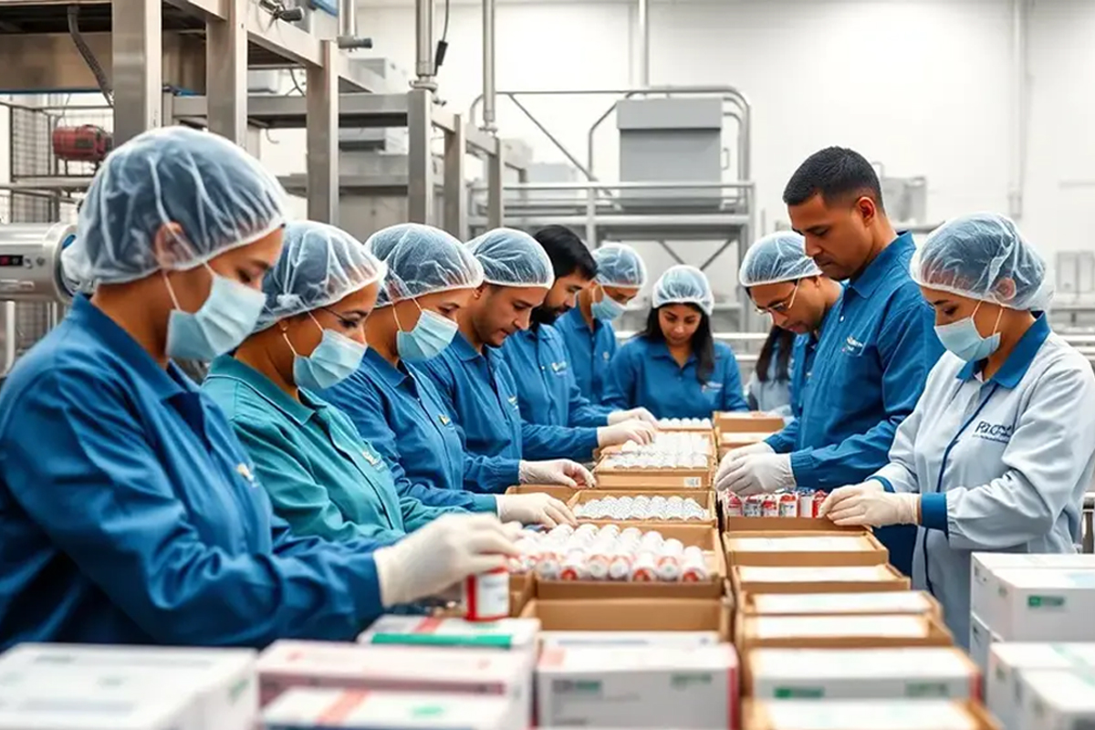
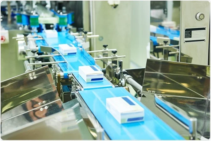
When the wafer is complete, it is cut into individual chips, or dice. Each chip undergoes rigorous electrical testing; defective ones are marked for removal. Surviving chips are packaged: mounted on a substrate, connected with ultra‑thin wires, and encased in a protective shell. This packaging ensures the chip can withstand heat, shock, and long‑term use, ready to power our digital world.
Challenges in Modern Chip Making
As chips approach atomic scales, physical limits become daunting. Quantum effects cause current leakage and heat buildup, challenging traditional designs. Solutions include new materials like wide‑bandgap semiconductors and advanced packaging that stacks components vertically. The global semiconductor supply chain remains fragile – geopolitical tensions, natural disasters, and pandemics can disrupt production. Companies are diversifying suppliers and investing in regional hubs to build resilience. The talent gap is another hurdle, prompting partnerships between companies and universities to train the next generation of engineers.
Economic Shifts and Regionalization
Governments worldwide are pouring billions into domestic chip fabrication facilities, offering tax incentives and subsidies to reduce dependence on foreign suppliers. This new era of investment aims to create self‑sufficient local ecosystems. At the same time, export controls and trade policies are fragmenting the global supply chain, forcing companies to adapt through nearshoring and reshoring. Strategic regionalization is reshaping where chips are made and how they flow to markets.
Innovations: Advanced Packaging and New Materials
With traditional scaling slowing, advanced packaging has emerged as a game‑changer. Techniques like 3D stacking and 2.5D integration use through‑silicon vias to connect multiple layers, dramatically reducing signal latency and power consumption. Heterogeneous integration combines specialized chiplets – each optimized for a specific task – into a single package, enabling tailor‑made solutions for AI, 5G, and automotive applications. New materials such as advanced ceramics and thermal compounds manage the heat generated by densely packed components.
Industry Players: Tech Giants vs. Startups
Large corporations like Intel, TSMC, and Samsung dominate chip fabrication due to the enormous capital required for cutting‑edge fabs. Their vertical integration allows them to design and produce custom chips at scale. However, startups and smaller firms contribute disruptive ideas in design, specialty materials, and packaging. Competition between giants and newcomers fuels rapid innovation across the industry.
Frequently Asked Questions
What is the significance of Moore’s Law in chip manufacturing?
Moore’s Law, coined by Gordon Moore in 1965, observes that the number of transistors on a microchip doubles roughly every two years while costs halve. This principle has driven the semiconductor industry to continually shrink transistors, resulting in more powerful and efficient chips. It remains a benchmark for progress, pushing companies to innovate relentlessly.
How does photolithography contribute to integrated circuit production?
Photolithography transfers circuit patterns onto a silicon wafer using light and a mask. It enables the precise placement of billions of transistors on a single chip, making complex integrated circuits possible. Without this technique, modern electronics would not exist.
What role does advanced packaging play in semiconductor development?
Advanced packaging encases and interconnects chips to boost performance and efficiency. It allows for greater integration of different chip types, better thermal management, and higher power densities. This facilitates continued advancement of technologies like AI, 5G, and IoT.
How do supply chain dynamics impact the chip industry?
The chip supply chain is complex and vulnerable to material shortages, geopolitical tensions, and logistics issues. Disruptions can delay production and raise costs. Strategic planning, diversification, and regionalization are essential to meet growing demand and maintain stability.